In the vast and ever-evolving world of electronics, latches play a critical role in Data and Control Systems, enabling information storage, circuit operation control, and seamless data transfer. Latches, often referred to as flip-flops, are fundamental components in digital circuit design, acting as memory elements that store binary data and ensure the sequential execution of tasks. Understanding the different types of latches is essential for electronics enthusiasts, students, and professionals seeking to master digital systems and computer architecture.
This article serves as a comprehensive guide to the various types of latches and their significance in electronics. We will explore their functionality, applications, and the unique features that distinguish them. From basic SR (Set-Reset) latches to advanced D, JK, and T flip-flops, we’ll examine their internal mechanisms, input/output characteristics, and the role of clock signals in their operation.
Along the way, we’ll also touch on related concepts such as types of memory and types of memory modules, as latches often work alongside these components to enable data retention and processing in digital systems. Additionally, we will explore how latches integrate with types of comparators and types of codecs in electronics to create robust and efficient data and control systems.
By gaining a clear understanding of the types of latches, you’ll be equipped with the knowledge to design effective digital circuits or troubleshoot existing systems. Whether you are a student studying digital electronics, a hobbyist exploring circuitry, or a professional working in the field, this guide aims to provide valuable insights into the indispensable role of latches in modern electronic systems.
Join us on this enlightening journey as we unravel the mechanisms of latches and uncover their diverse applications, showcasing why they remain a cornerstone of digital electronics in today’s technological landscape.
Boost operational efficiency with LinkSemi’s Excess Electronic Components Solution, designed to optimize inventory sales and reduce excess costs. Our AI-powered insights and automated workflows provide significant Cost Savings in Electronic Components procurement. Additionally, our advanced Electronic Component Shortage Module addresses supply chain challenges, ensuring seamless production and maintaining consistent operational performance.
Different Types of Latches
Here is a list of different types of latches, along with a short description for each:
- SR (Set-Reset) Latch: The SR latch is a basic latch that stores a single bit of information and has two inputs, the Set (S) and Reset (R) signals. It can be constructed using NOR or NAND gates and has a simple operation where one input sets the latch to “1” and the other input resets it to “0.”
- D Flip-Flop: The D flip-flop, also known as the data flip-flop, stores a single bit of information and has a single input called the “Data” (D) input. It is edge-triggered and transfers the input data to the output on the rising or falling edge of a clock signal.
- JK Flip-Flop: The JK flip-flop is an extension of the SR latch with an additional feature. It has two inputs, J (Jump) and K (Kill), and behaves like an SR latch when both inputs are high. However, it also has a “toggle” mode where the output switches state on each clock edge when both J and K inputs are low.
- T Flip-Flop: The T flip-flop, also known as the toggle flip-flop, is a modification of the JK flip-flop. It has a single input called the “Toggle” (T) input and toggles its output state (0 to 1 or 1 to 0) on each rising or falling edge of the clock signal, depending on the state of the T input.
- Master-Slave Flip-Flop: The master-slave flip-flop consists of two interconnected flip-flops, typically D or JK flip-flops. It operates in two phases: the master phase and the slave phase. The master flip-flop captures the input data while the slave flip-flop holds the output stable until the next clock cycle.
- Transparent Latch: Transparent latches, also known as level-sensitive latches, are latching circuits that allow the input to pass to the output when the latch enable signal is active (typically high). They can be implemented using simple logic gates and are useful for storing data continuously as long as the latch enable signal remains active.
- Gated D Latch: The gated D latch is similar to the transparent latch but with an additional input called the “Enable” input. The latch stores the input data when the enable signal is active, and it holds the stored value when the enable signal is inactive.
- Edge-Triggered Latch: Edge-triggered latches, such as the D flip-flop, JK flip-flop, and T flip-flop, respond to specific edges (rising or falling) of a clock signal. They capture and retain the input data at the moment of the triggering edge and update the output accordingly.
These are some of the commonly used types of latches in electronics. Each type has its own unique characteristics, applications, and advantages, making them suitable for different scenarios in digital circuit design and sequential logic operations.
SR (Set-Reset) Latch
The SR latch, also known as the Set-Reset latch, is one of the basic building blocks in digital electronics. It serves as a memory element, capable of storing a single bit of information. The SR latch has two inputs, Set (S) and Reset (R), which control its behavior. In this section, we will explore the working principle, truth table, and applications of the SR latch.
Working Principle
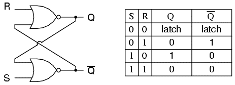
The SR latch can be constructed using NOR gates or NAND gates. Let’s consider the NOR gate implementation for our discussion. The SR latch has two cross-coupled NOR gates connected in a feedback arrangement. The output of one gate is connected to the input of the other gate, and vice versa.
- Set (S) Input: When the Set input is activated (high), it sets the output of one NOR gate to logic level 0 (low). This causes the output of the other NOR gate to become logic level 1 (high), storing the “set” state.
- Reset (R) Input: When the Reset input is activated (high), it sets the output of the other NOR gate to logic level 0 (low). Consequently, the output of the first NOR gate becomes logic level 1 (high), storing the “reset” state.
- Stable State: When neither the Set nor the Reset inputs are activated (both low), the feedback arrangement maintains the latch in its stable state, retaining the previously stored value.
Truth Table
The behavior of an SR latch can be summarized using a truth table:
![]()
In the truth table, “Previous” refers to the previous state stored in the latch, and “Unstable” indicates an indeterminate state that can occur when both Set and Reset inputs are activated simultaneously.
Applications
SR latches find applications in various digital systems and circuits. Some common uses include:
- Control Circuitry: SR latches are often used as control elements in sequential logic circuits, such as state machines and counters, to store and synchronize data.
- Memory Units: They serve as basic memory elements in larger memory units, such as registers, where multiple SR latches are combined to store and manipulate binary data.
- Bistable Operations: The SR latch’s ability to hold a stable state makes it suitable for bistable operations, such as toggling or latching operations.
- Pulse Stretching: SR latches can be used to stretch the duration of a pulse, where a short input pulse can be extended and held for a longer period.
D Flip-Flop
A D flip-flop, also known as a data flip-flop, is a fundamental type of sequential logic circuit. It is widely used in digital electronics for storing and transferring a single bit of data. The D flip-flop operates based on the rising or falling edge of a clock signal, making it an edge-triggered device. Let’s explore the D flip-flop in detail, including its working principle, truth table, and applications.
Working Principle
The D flip-flop consists of a data input (D), clock input (CLK), and output (Q). It stores the input data (D) and transfers it to the output (Q) based on the clock signal. When the clock signal transitions from low to high or high to low (depending on the flip-flop’s specific configuration), the D flip-flop captures the data input and updates the output.
Truth Table
The truth table of a D flip-flop showcases its behavior based on different input combinations. Here is the truth table for a positive-edge-triggered D flip-flop:
![]()
In the truth table, Q(t) represents the output at time t, and Q(t+1) represents the output at the next clock cycle.
Functionality
The D flip-flop stores the input data (D) when the clock signal transitions from low to high (positive edge) or high to low (negative edge). It maintains the stored data until the next clock edge, where it updates the output with the new input data. The D flip-flop is known for its simplicity and is often used as a building block for more complex sequential logic circuits.
Applications
The D flip-flop finds extensive usage in various applications, including:
- Memory circuits: In computer memory systems, D flip-flops are crucial for storing binary data in registers and memory cells.
- Shift registers: D flip-flops are employed in shift register circuits to enable the sequential shifting of data bits.
- State machines: D flip-flops play a vital role in the implementation of state machines, which are used in various digital systems for controlling and sequencing operations.
- Clock synchronization: D flip-flops are utilized for synchronizing signals in circuits to avoid timing issues and ensure proper data transfer.
- Frequency division: D flip-flops can be employed to divide the frequency of a clock signal by 2, making them useful in frequency dividers and counters.

JK Flip-Flop
The JK flip-flop is a widely used sequential logic circuit in digital electronics. It is an extension of the SR (Set-Reset) latch with an additional feature that overcomes some of the drawbacks of the SR latch. The JK flip-flop offers versatility and flexibility in various applications, making it an essential component in digital systems. Let’s explore the JK flip-flop in detail.
Overview
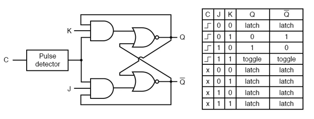
The JK flip-flop is named after its two inputs, J (Jump) and K (Kill). It behaves like an SR latch when both inputs are high. However, it introduces a “toggle” mode when both J and K inputs are low, allowing the output state to toggle on each clock edge. The JK flip-flop combines the functionalities of the SR latch and the T flip-flop, providing more control and functionality in sequential logic operations.
Functionality
- Set State: When the J input is high (1) and the K input is low (0), the JK flip-flop enters the set state. This sets the output to high (1) regardless of the current state.
- Reset State: Conversely, when the K input is high (1) and the J input is low (0), the JK flip-flop enters the reset state. This resets the output to low (0) regardless of the current state.
- Toggle State: When both J and K inputs are low (0), the JK flip-flop operates in the toggle mode. In this mode, the output state toggles (changes from 0 to 1 or from 1 to 0) on each rising or falling edge of the clock signal, depending on the current state.
Truth Table
The behavior of a JK flip-flop can be represented by a truth table:
![]()
Q(t) represents the current state, and Q(t+1) represents the next state.
Timing Diagram
A timing diagram visually represents the behavior of a JK flip-flop concerning the clock signal and input transitions. It illustrates how the output state changes based on the input values and clock edges.
Applications
The JK flip-flop finds extensive applications in digital systems, including:
- Frequency Division: It is used in frequency division circuits, such as binary counters and frequency dividers.
- State Machines: The JK flip-flop is a fundamental building block in designing state machines, which are used in control systems, data processing, and communication protocols.
- Registers and Shift Registers: It is employed in the construction of registers and shift registers, facilitating data storage and shifting operations.
T Flip-Flop
The T flip-flop, also known as the toggle flip-flop, is a fundamental sequential logic device widely used in digital circuit design. It is a modification of the JK flip-flop and offers a simple and efficient way to toggle the state of its output based on the input and clock signals. In this section, we will explore the T flip-flop’s working principle, truth table, and applications.
Working Principle
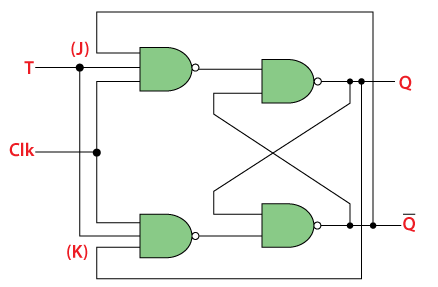
The T flip-flop operates on the basis of a single input called the “Toggle” (T) input. The T input determines whether the flip-flop’s output state will toggle (change from 0 to 1 or 1 to 0) or remain the same upon each rising or falling edge of the clock signal, depending on the flip-flop’s configuration.
Truth Table
The truth table for a T flip-flop showcases its behavior based on different combinations of inputs and clock signals:
![]()
From the truth table, we can observe that when the T input is 0, the flip-flop’s output remains unchanged, while when the T input is 1, the output toggles (flips) on each rising edge of the clock signal.
Applications
The T flip-flop finds applications in various digital systems, including:
- Frequency Division: The T flip-flop can be used as a frequency divider. By feeding a specific clock frequency to the T input, the flip-flop can generate an output frequency that is half (or a fraction) of the input frequency.
- Digital Counters: T flip-flops are key building blocks in the design of digital counters, such as binary counters or modulo-N counters. By cascading multiple T flip-flops together, it becomes possible to count and represent numbers in binary or other numeral systems.
- State Machines: T flip-flops are vital components in the implementation of sequential logic circuits and finite state machines. They help in storing and transitioning between different states based on the input conditions and clock signals.
Master-Slave Flip-Flop
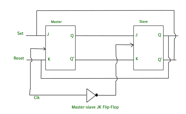
The master-slave flip-flop is a type of sequential logic device commonly used in digital circuit design. It consists of two interconnected flip-flops, typically D or JK flip-flops, operating in a master-slave configuration. In this section, we will explore the working principle, timing diagram, and applications of the master-slave flip-flop.
Working Principle
The master-slave flip-flop operates in two distinct phases: the master phase and the slave phase. During the master phase, the master flip-flop captures the input data based on the clock signal‘s rising or falling edge. The captured data is then transferred to the slave flip-flop during the slave phase. This configuration ensures that the output remains stable and unaffected by the input during the master phase.
Timing Diagram
A timing diagram illustrates the behavior of a master-slave flip-flop based on the input signals and clock edges. The diagram showcases the relationship between the clock, input, and output signals over time, highlighting the master and slave phases.
_______ _______ _______
CLK ____| |_______| |_______| |_____
DATA ______________X_______| |_______| |___
OUTPUT ________________X______| |_______| |_
In the timing diagram:
- CLK represents the clock signal, with rising or falling edges triggering the master-slave flip-flop operation.
- DATA represents the input data to be captured by the master flip-flop during the master phase.
- OUTPUT represents the stable output of the master-slave flip-flop, reflecting the data transferred from the master to the slave flip-flop during the slave phase.
Applications
The master-slave flip-flop finds applications in various digital systems, including:
- Synchronization: The master-slave configuration helps to eliminate timing issues and ensure proper synchronization between the input data and clock signal, making it suitable for high-speed and reliable operation.
- Sequential Circuits: Master-slave flip-flops are commonly used in the design of sequential circuits, such as registers and shift registers, where the output needs to be stable between clock cycles.
- Frequency Division: By cascading multiple master-slave flip-flops, it is possible to divide the frequency of the input clock signal, enabling frequency division in applications like frequency synthesizers or frequency dividers.
Transparent Latch
A transparent latch, also known as a level-sensitive latch, is a sequential logic device widely used in digital circuit design. It offers a straightforward way to store and hold data, allowing the input to pass through to the output when the latch enable signal is active. In this section, we will explore the working principle, truth table, and applications of the transparent latch.
Working Principle
The transparent latch operates based on a latch enable signal and the data input. When the latch enable signal is active (typically high), the transparent latch is “transparent,” meaning that the input data passes directly to the output. Conversely, when the latch enable signal is inactive (low), the latch holds the last captured data, keeping the output stable.
Truth Table
The truth table for a transparent latch showcases its behavior based on the input data and latch enable signal:
![]()
From the truth table, we can observe that when the latch enable signal is 0, the output holds its current state (Q(t)). When the latch enable signal is 1, the output matches the input data.
Applications
The transparent latch finds applications in various digital systems, including:
- Data Storage: Transparent latches are commonly used as temporary data storage elements, allowing the data to flow through when the latch enable signal is active. This feature is useful in buffering or latching data before it is processed or transferred to other components.
- Signal Conditioning: Transparent latches can be used for signal conditioning applications where data integrity and stability are crucial. By controlling the latch enable signal, the input data can be reliably captured and held until further processing.
- Address Decoding: Transparent latches are utilized in address decoding circuits, where they capture and hold specific address signals until the decoding process is complete.
Gated D Latch
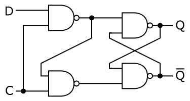
The gated D latch is a sequential logic device widely used in digital circuit design. It is a fundamental latch that combines a D flip-flop with an additional input called the “Enable” (EN) input. The gated D latch allows the input data to be stored when the enable signal is active, and it holds the stored value when the enable signal is inactive. In this section, we will explore the working principle, truth table, and applications of the gated D latch.
Working Principle
The gated D latch operates based on the D input, the enable (EN) input, and the clock signal. When the enable signal (EN) is active (typically high) and the clock signal is triggered, the D latch captures and stores the D input value. The stored value remains unchanged when the enable signal goes inactive or the clock signal is not triggered.
Truth Table
The truth table for a gated D latch showcases its behavior based on the input data (D), enable signal (EN), and clock signal:
![]()
From the truth table, we can observe that when the enable signal (EN) is inactive (0), the output (Q) holds its previous state (Q(t)). When the enable signal (EN) is active (1) and the clock signal triggers a rising edge, the output (Q) matches the input data (D).
Applications
The gated D latch finds applications in various digital systems, including:
- Memory Elements: Gated D latches are used as basic memory elements for temporary data storage in digital circuits. They provide the ability to latch and hold data, allowing for further processing or transfer.
- Control Circuitry: Gated D latches are commonly utilized in control circuitry, where they enable or disable certain functions based on the control signals. The enable signal (EN) acts as a gate, controlling the flow of data or operations.
- Synchronous Systems: Gated D latches are suitable for synchronous systems, where the enable signal is synchronized with the clock signal. They ensure that the stored data remains consistent and synchronized with the overall system operation.

Edge-Triggered Latch
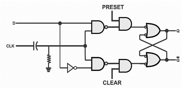
The edge-triggered latch, also known as a flip-flop, is a fundamental sequential logic device widely used in digital circuit design. It operates based on specific edges (rising or falling) of a clock signal, allowing the input data to be captured and retained at the moment of the triggering edge. In this section, we will explore the working principle, truth table, and applications of the edge-triggered latch.
Working Principle
The edge-triggered latch is controlled by a clock signal and operates in two distinct phases: the capture phase and the hold phase. During the capture phase, the input data is sampled and stored based on a specific edge (rising or falling) of the clock signal. The stored data is then held and remains unchanged during the hold phase until the next triggering edge of the clock signal
Truth Table
The truth table for an edge-triggered latch showcases its behavior based on different combinations of input data and clock signals:
![]()
From the truth table, we can observe that the output (Q) of the edge-triggered latch reflects the stored data (Q(t)) until the triggering edge of the clock signal occurs. At that moment, the output (Q) changes to the new captured data (Q(t+1)).
Applications
The edge-triggered latch finds applications in various digital systems, including:
- Storage Elements: Edge-triggered latches serve as key building blocks for various storage elements, such as registers and memories. They enable the reliable and synchronized storage of data in sequential logic circuits.
- Data Synchronization: Edge-triggered latches are essential in systems where data synchronization is crucial. By capturing and holding the input data based on a specific edge of the clock signal, they ensure consistent and synchronized data handling.
- State Machine Design: Edge-triggered latches play a vital role in the design and implementation of state machines. They help in capturing and transitioning between different states based on the clock signal and input data.
Conclusion
In summary, understanding the different types of latches is crucial in the field of electronics. From the versatile SR latch to the data-capturing D flip-flop, the synchronization-friendly master-slave flip-flop, and more, each type of latch offers unique functionality and applications. By comprehending their working principles, truth tables, and uses, one can confidently navigate digital circuit design and troubleshooting. Whether you’re a hobbyist or a professional, the knowledge of latches empowers you to unleash the potential of electronics, tackle complex projects, and contribute to this ever-evolving field.
FAQs about Types of Latches
- What are latches in electronics?
Latches are fundamental building blocks in digital circuit design that store and retain information, control circuit operations, and facilitate data transfer.
- How many types of latches are there?
There are several types of latches, including the SR latch, D flip-flop, JK flip-flop, T flip-flop, and transparent latch, each with its own unique characteristics and applications.
- What is the difference between a latch and a flip-flop?
While both latches and flip-flops are sequential logic devices, the main difference lies in their triggering mechanisms. Latches are level-sensitive and continuously update their outputs based on the input, while flip-flops are edge-triggered and capture the input at specific clock signal edges.
- What are some common applications of latches?
Latches find applications in various digital systems, such as frequency division, digital counters, state machines, data storage, signal conditioning, and address decoding, to name a few.
- Why is understanding the types of latches important?
Understanding the types of latches is crucial for digital circuit designers as it allows them to make informed decisions, troubleshoot issues, and design circuits that meet specific requirements. Having knowledge of latches empowers individuals to effectively utilize them in various electronics projects.
